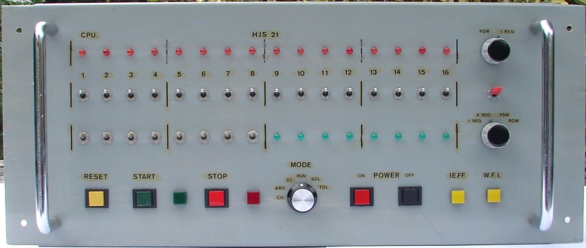
The first drawing I made was the CPU front panel which dates back to the 29th of February 1976. I was forced to make this drawing by my
school teacher before he allowed me to use the school workshop to make the front panel.
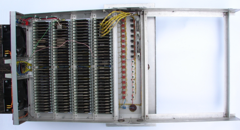
From a earlier attemp to built a computer I learned that the hardware construction must allow to make easy changes and that it mustn't become a mess.
This was the result after some attemps:
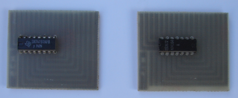
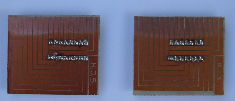
- every TTL chip is soldered on his own PCB.
- each PCB is inserted in a 18 pins connector. I had to etch these PCB's myself.
Pin 1 till 14 or 16 of the TTL chip was connected with pin 1 -14/16 of the connector.

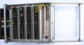
Left a 16 pins and right a 14 pins TTL chip. The backside of the PCB's shown in the left pictures
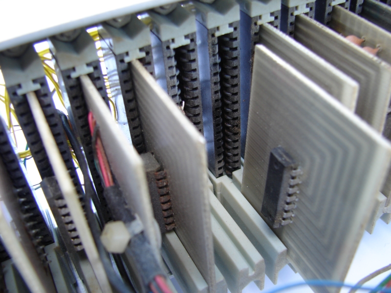
These two pictures gives a good idea how the whole logic hardware is built up in the HJS22.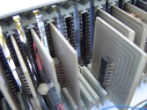
After alot of changes it still look clean and orderly. I didn't use wirewrap technology because I didn't know it existed at the time.
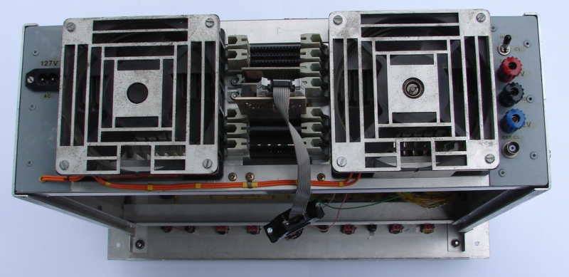
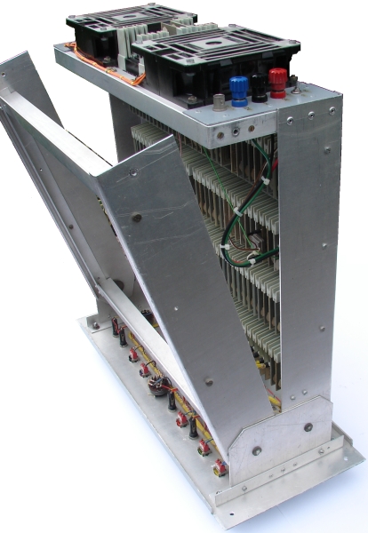
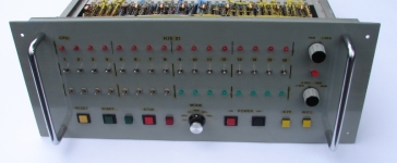
The whole mechanical contruction of the can best been seen in these pictures:

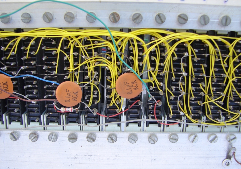
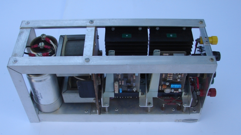
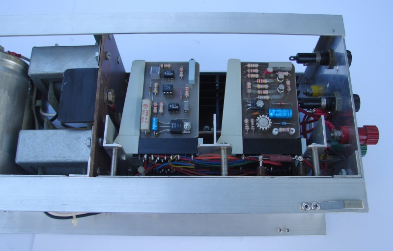
Here are some pictures of the dual +5V switching power supply, including Over Voltage Protection, which I build to supply
the CPU and the I/O unit.